|
|
|
|
 |
 |
|
| Special Product Type: |
| Carbon Paste Through Hole |
| Silver Through Hole |
| Electroless Nickel And Immersion gold |
| Immersion Silver |
| Immersion Tin |
| Heavy Copper Board |
| Chip On Board |
| Impedance Control And High Frequency Board |
| High Density Interconnection |
| Engineering Capability and Order Lead Time |
| Items |
Min Lines Width/Spacing |
Min Holes Size |
Sample lead Time
(Day) |
Mass Production Lead Time (Day) |
| 4 Layered Board |
0.1mm |
0.25mm |
5-7 |
7-10 |
| 6 Layered Board |
0.1mm |
0.25mm |
7-14 |
14 |
| 8 Layered Board |
0.1mm |
0.25mm |
7-14 |
15 |
| 10 Layered Board |
0.1mm |
0.25mm |
7-14 |
15 |
| 12 Layered Board |
0.1mm |
0.25mm |
7-14 |
15 |
| 14 Layered Board |
0.1mm |
0.25mm |
7-14 |
15 |
| Input/Output Files Format |
| GERBER Files |
Drill/Rout |
Fabrication Drawings |
Network |
| ODB++ (Genesis 2000) |
Excellon1 |
HPGL |
IPC-D-350 |
| Gerber |
Excellon2 |
DXF |
IPC-D-356(A) |
| Gerber RS274X |
Hitachi |
PDF |
ATF |
| DPF |
Turdrill |
Post Script |
/ |
| Using Tools |
| Items |
Names |
Quantities |
| MI Software |
Inplan |
2 |
| CAM Software |
UCAM |
10 |
| Genesis 2000 |
17 |
| Plot |
Barco |
3 |
| Technology Roadmap |
| Process |
Features and Capability |
Unit |
2012 |
2013 |
| Material |
TG |
.C |
130-180 |
130-200 |
| Halogen Free |
- |
Yes |
Yes |
| Anti-CAF material |
- |
Yes |
Yes |
| Flammability |
- |
94V-0 |
94V-0 |
| Board Dimension |
Max Panel Size |
Inch |
21.5*24.5 |
21.5*24.5 |
| mm |
546*622 |
546*622 |
| Max Finished Board Size |
Inch |
19.5*22.5 |
20*23 |
| mm |
495*572 |
508*584 |
| Min Board Thickness |
mm |
0.4 |
0.3 |
| Max Board Thickness |
mm |
3.0 |
3.4 |
| Inner Layer |
Min Line Width./Space |
mil |
3.5/3.5 |
3/3 |
Max Copper Thickness
(Width/Space) |
OZ |
4 |
5 |
| mil |
8/8 |
10/10 |
| Min Core Thickness |
mm |
0.075 |
0.05 |
| Lamination |
Max Layer Count |
Layer |
12 |
16 |
| Min Dielectric Thickness |
mil |
3 |
2.8 |
| Ply Up of Prepregs |
Ply |
3 |
4 |
| Layer to Layer Registration |
mil |
4 |
3 |
| Drilling |
Min Mechanical Drill Size |
mm |
0.2 |
0.2 |
| Min Hole to Hole Pitch |
mm |
0.55 |
0.5 |
| Min Laser Drill Size |
mm |
0.1 |
0.08 |
| Buried via & Blind Via |
- |
Yes |
Yes |
| Outer Layer |
Min Line Width/Space |
mil |
3.5/3.5 |
3/3 |
Max Copper Thickness
(Width/Space) |
OZ |
4 |
5 |
| mil |
10/10 |
12/12 |
| Plating |
Aspect Ratio |
ratio |
8:1 |
10:1 |
| Max Copper Thickness of Min Hole |
mil |
0.8 |
1 |
| Solder Mask |
Min S/M Thickness |
mil |
0.4 |
0.4 |
| S/M Registration Tolerance |
mil |
3 |
2 |
| Min Solder Dam Width |
mil |
2 |
2 |
| Others |
Impedance Control |
ohms |
37-120 |
37-120 |
| Impedance Control Tolerance |
% |
10% |
8% |
Application of Products
| Industry |
Major Application of the Group’s products |
 Electronic Products Electronic Products |
Plasma TV, LCD TV, CRT TV, DVD Player, DVD Recorder, Air Conditioner, Camera |
| Computers and Computer Peripherals |
Mother Board, Networking Device, Printer, Cable TV, HDD, CD-Rom |
| Communications Equipment |
Cordless Phone, Mobile Phone, Mobile Phone Accessories, Fax Machine |
|
|
|
|
 |
|
|
|

 LED Products
PCB Products
Quality
Sales Network
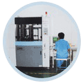
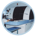
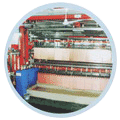
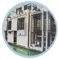
Production Facilities
Environmental Protection
Research & Development
LED Products
PCB Products
Quality
Sales Network
Production Facilities
Environmental Protection
Research & Development